A new way of producing semiconductors using vertical transistors could be a gamechanger for computers, with IBM and Samsung claiming it may even result in phone batteries that last up to a week.
In a joint announcement, IBM and Samsung said they had reached a “breakthrough” with vertical transistor architecture that early experiments have found reduces energy usage by 85 per cent compared to existing technologies.
The key to unlocking this energy efficiency are vertical transport field effect transistors (VTFET) – for which IBM holds a patent – that allow for more transistors to be fit into increasingly smaller spaces and less energy lost to the environment.
“Historically, transistors have been built to lie flat upon the surface of a semiconductor, with the electric current flowing laterally, or side-to-side, through them,” IBM said.
VTFET’s, on the other hand, “are built perpendicular to the surface of the chip with a vertical, or up-and-down, current flow” which IBM said “addresses many barriers to performance and limitations to extend Moore's Law”.
As components get smaller and smaller, chip manufacturers are coming against hard limits to Gordon Moore’s projection that the number of transistors on an integrated circuit would double every two years.
Francesca Iacopi is a Professor of Electronics in the Faculty of Engineering and IT at the University of Technology Sydney.
She told Information Age that the idea of using vertical transistors to fit more of them onto a silicon chip isn’t new in and of itself but the actual fabrication of a wafer using VTFETs is an important step to keeping up with Moore’s Law.
“At the moment the lateral approach to transistors are getting about as small as we can ever get,” Professor Iacopi said.
“At these size you have problems with leakage and dissipation, so if you don’t control the channel field uniformly, the voltage you put into the system leaks out and isn’t used for computation.
“There is no doubt vertical transistors are moving in the direction to make chips more efficient and reduce energy overall consumption.”

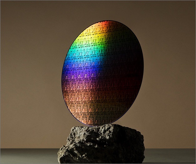
A vertical transport field effect transistor (VTFET) wafer. Image: supplied
But does that mean Samsung’s next generation of smart phones will go a whole week without needing to be charged?
“I would be very careful with those statements,” Professor Iacopi told Information Age.
“Of course there will be an improvement but exactly how much of one, and if it will last a week, I’m not so sure.”
Still, the demonstration that IBM and Samsung can fabricate chips using VTFETs certainly paves the way for new possibilities in computation.
“On the plane, the real estate is very expensive,” Professor Iacopi said about horizontal, planar transistors.
“In 3D you can go higher so there is more latitude to make different configurations. I didn’t see anything in the announcement about stacking transistors, but potentially why not?
“It will all depend on how complicated the fabrication process becomes and how much more it will cost.”


