
Microprocessor design is set for its biggest shakeup in decades, after Intel debuted new glass substrates that are expected to help the chip-making industry reach its stretch goal of squeezing 1 trillion transistors onto a chip by 2030.
Substrates – the part of a CPU onto which microscopic ‘traces’ are etched in a process called photolithography – are crucial to the integrity of any microprocessor, since they provide the foundation on which the rest of the chip operates.
Silicon has been favoured for decades, but the material has increasingly run into challenges such as warping from the immense amounts of heat created by ever denser microprocessors and ever narrower metal traces that connect their elements.
Narrower traces enable CPUs to run faster but they can’t dissipate heat as effectively, impeding the flow of electricity and potentially causing the silicon to warp and expand as cooling becomes increasingly difficult.
This has forced chipmakers to explore other options as Moore’s Law – the long-held principle that improvements in microprocessor technology will double the number of transistors in a chip every two years – runs into fundamental physical constraints.
Enter glass substrates – an alternative material that, Intel says, can tolerate higher temperatures, have “ultra-low flatness” to improve the accuracy of lithography, offer 50 per cent less pattern distortion, and have “dimensional stability” that allows layers of transistors to be placed on top of each other with pinpoint accuracy.
The new technology – which is being hailed as a way to revive Moore’s Law – has delivered “industry-leading glass substrates for advanced packaging… that will benefit our key players and foundry customers for decades to come,” said Babak Sabi, Intel senior vice president and general manager of Assembly and Test Development as the new technology was announced.
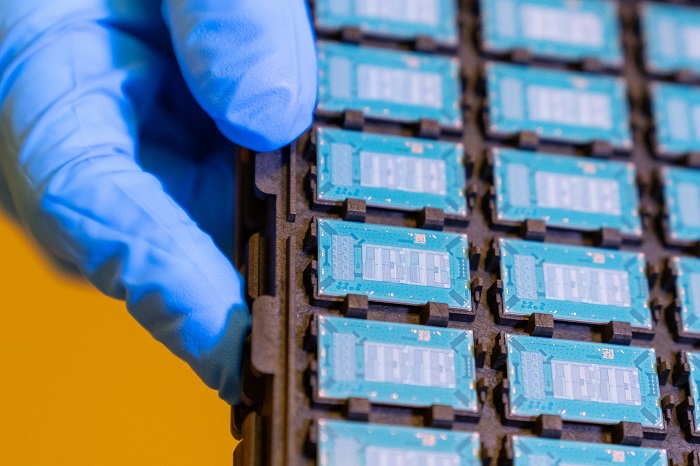
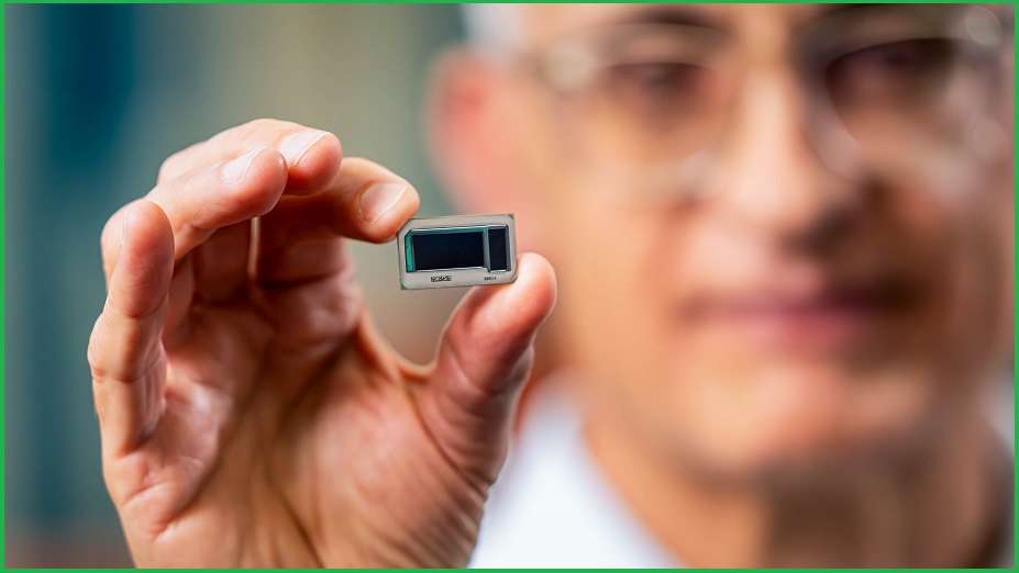
Intel has already started producing glass substrate test units. Image: supplied
Use of the substrates during CPU ‘packaging’ – the process by which the many elements of a microprocessor are assembled and fixed into place – will allow future designs to pack ever more transistors while remaining more structurally stable than those built on silicon packaging.
Because it enables the increasingly accurate positioning of traces connecting the various parts of a CPU, what Intel calls the “viable and essential” glass design will also improve internal communications speed – increasing performance dramatically and allowing chips to communicate over optical connections.
These and other capabilities “allow for better power delivery solutions while achieving high-speed signaling that is needed at much lower power,” Intel said. “These many benefits bring the industry closer to being able to scale 1 trillion transistors on a package by 2030.”
That’s far beyond current consumer chips such as Apple’s M2 Ultra desktop CPU, which has 134 billion transistors and uses internal wiring just 5 nanometres wide – a feat of miniaturisation that highlights just how important efficient chip design will be to breathing new life into Moore’s Law.
Bigger, better, faster, smaller
Intel isn’t the only company developing glass substrate solutions: Japanese firm Dai Nippon Printing, for one, outlined a glass core substrate (GCS) solution that, the company says, offers chip designers freedom to balance thickness, warpage, stiffness, and smoothness.
As the microprocessor market rapidly incorporates the technology into real chips – Intel has promised “complete glass substrate solutions” by the second half of this decade – the new architecture will be indispensable for developing next-generation processors for applications such as artificial intelligence (AI) and ‘hyperscale’ cloud operators.
Systems built on the chips – including increasingly complex designs that integrate multiple ‘chiplets’ into a single integrated package – will be particularly valuable in the growing number of data centres that are being filled with servers to support rapidly expanding use of such applications.
Australian data centre giant Macquarie Data Centres, for one, recently announced that it will significantly expand its Macquarie Park Data Center Campus in Sydney from 10MW of capacity to 50MW – at which point it will, the company claims, “become the most advanced data centre in Sydney” – as well as expanding the capacity of its IC3 Super West facility by up to 41 per cent, to 45MW of computing capacity.
Such “advanced AI-ready data centres” will be crucial to supporting corporate, government, and industry use of AI – and they will require ever more efficient CPU technology to provide unprecedented amounts of compute power, as well as air and liquid cooling technologies to avoid an operational meltdown.
“Unlocking the full potential of AI hinges on the availability of AI-ready data centres,” Macquarie Data Centres group executive David Hirst said, adding that “to ensure optimal performance in training and inference of these AI models, we are designing our upcoming data centres to meet and surpass the demanding requirements for higher densities.”