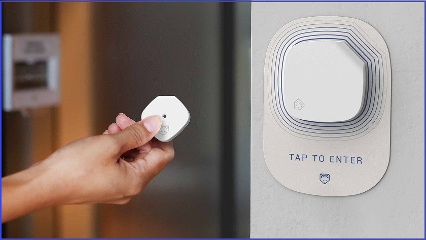
A new biosensor developed by RMIT researchers can detect COVID-19 when placed in a room or worn as a personal tag.
The Soterius Scout sensor is sensitive enough to detect the presence of tiny amounts of the SARS-CoV-2 virus and has results within a minute to provide the all-clear for someone to enter a work environment or alert them if they need to undertake a medical COVID test and self-isolate.
Scout uses nanotechnology-enabled biosensors developed at the RMIT Micro Nano Research Facility in Melbourne.
One sensor can detect up to eight viral strains and be adapted to detect new variants or novel viruses as they emerge.
After a successful prototype, RMIT and Soterius in partnership with MIP Diagnostics, the Burnet Institute, D+I and Vestech, are working towards a commercial release early 2022.
Professor Sharath Sriram, RMIT University project lead, told Information Age the high-tech sensor uses semiconductors, the same as those used in electronics that give or remove charge, with a surface coated with locations where the virus would bind.
“These are designed carefully to match the target – it has to be designed to be a perfect match for accurate readings and precise measurements,” said Sriram.
“The analogy is a pair of jigsaw puzzle pieces – only the right pieces would fit into each other. So, if the virus (or any target) is present, they will go into their matching site. We measure the electrical properties of a specially-designed semiconductor surface,” he says.
When the target material lands, it changes the electrical property of the device, which instantly reveals whether the target virus is present or not (a positive or negative charge). "More importantly, there are millions of target sites – as more are occupied, the strength of the electrical signal changes. This allows us to estimate concentration of the target reliably,” he says.

The Soterius Scout team [L to R]: Professor Sharath Sriram (RMIT), Dr Alasdair Wood (Soterius), Dr Md Ataur Rahman (RMIT), Dr Chih Wei Teng (Soterius), Dr Ganganath Perera (RMIT)
The power of ultraviolet light processes
The high-tech sensor utilises a system with three parts – the sensor chip, the flexible electronics using micro-fabrication and the reader (just a standard NFC-enabled smartphone or simple NFC readers available in the market).
The chip uses silicon electronics fabrication technology, the same as electronics in laptops and phones.
On the silicon wafer, the sensor is defined by a process called ‘photolithography’ (patterning with light), where ultraviolet light is used to define the micro-scale structure. “These are coated with thin (100nm, 1000x thinner than human hair) layers of gold, which defines the electronic interface,” Sriram said.
"On this electronic structure, the surface is chemically modified to define the binding sites for the target.
“In this particular case, we use synthetic nano-imprinted polymer molecules from MIP Diagnostics in the UK,” he says.
The interface uses flexible electronics which collect the sensor data and the antenna and peripherals that transmit the data are defined on a 25µm thick plastic sheet using a material called polyimide.
“We can either use laser patterning or etching to define the structures. On top of this, miniature electronic components (~0.2 mm is size) are assembled to form the circuit.”
The device prototypes are currently made in the Micro Nano Research Facility at RMIT University.
However, although it has the capacity to make large volume of sensor chips, the interface electronics volumes are limited.
“The objective is to manufacture in Victoria or Australia, with a few proposals submitted to government agencies to support such local manufacturing.”
Tiny technology with big potential
Despite its micro-size, the technology is versatile and can be rapidly repurposed to target any virus – providing a host of potential applications.
“The sensor chip can be covered with binding sites for any material of interest, be it other respiratory viruses, biomarkers related to disease or diet, or to find minor variants of DNA,” Sriram said.
The genius of this technology lies in its compact electronics – the size of a postage stamp and without a battery – that allows it to be deployed anywhere in the world, reaching remote and vulnerable communities.
“The devices have been developed with manufacturing requirements a primary consideration,” said Sriram.
“Every step used in production leverages existing manufacturing techniques, which creates opportunities to scale-up rapidly.”


